Discussion Qualcomm Snapdragon Thread

Page 39 - Seeking answers? Join the AnandTech community: where nearly half-a-million members share solutions and discuss the latest tech.

Ghostsonplanets

Senior member
Mar 1, 2024
338
544
96
I was reading some past Snapdragon rumors and just learned on a reddit post from @FlameTail that Phoenix M uses 1.1W. That's insanely low. I honestly wouldn't mind a Snap 7 Gen 4 with 6/8 Phoenix M + Adreno 820😃.
Some are speculating this is an event to announce the Snapdragon X Plus
Aye. And would match with SemiAccurate free snippet that QCOM wants to do an event for each new Snap X part that they announce.

If QCOM is able to slot Snap X Plus on <$1000 machines and have good availability, it will be a game changer on mainstream laptops.
 

FlameTail

Platinum Member
Dec 15, 2021
2,356
1,275
106
I was reading some past Snapdragon rumors and just learned on a reddit post from @FlameTail that
From Mr. Swords yes?
Phoenix M uses 1.1W. That's insanely low.
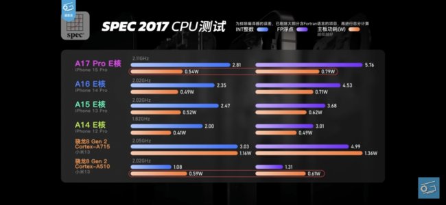
Not as insane as this:
Screenshot_20231002_052249_YouTube.jpg
The most efficient E-core in the world.
Aye. And would match with SemiAccurate free snippet that QCOM wants to do an event for each new Snap X part that they announce.
I WANT TO KNOW WHAT'A INSIDE THAT ARTICLE. I ma pretty sure it contains some information in additional to X Plus stuff.
If QCOM is able to slot Snap X Plus on <$1000 machines and have good availability, it will be a game changer on mainstream laptops.
Yes, that's where the majority of the volume is for laptop sales.

If Qualcomm wants to increase WoA marketshare rapidly, this is the way.
 

FlameTail

Platinum Member
Dec 15, 2021
2,356
1,275
106
This is a slide from last October
Snapdragon X Elite Pre-Briefing Deck 11.jpeg
And this is a much more recent slide:
Screenshot_20240404_070241_Chrome.jpg
Both are Geekbench 6 Multi-core, but in the new slide, the Snapdragon X Elite is consuming 10W less.

Is Qualcomm hiding something?
 

SarahKerrigan

Senior member
Oct 12, 2014
377
544
136
This is a slide from last October
View attachment 97278
And this is a much more recent slide:
View attachment 97279
Both are Geekbench 6 Multi-core, but in the new slide, the Snapdragon X Elite is consuming 10W less.

Is Qualcomm hiding something?

Or they've improved their DVFS curve as development continued. I don't think I'd conclude they're hiding something based on this - but, as always, assume that pre-release vendor claims are under the most favorable circumstances possible.
 

FlameTail

Platinum Member
Dec 15, 2021
2,356
1,275
106
Or they've improved their DVFS curve as development continued.
If that is indeed the case, that would be really impressive.

But I still think there's a gotcha somewhere. Maybe these new slides were prepared using the 23W reference laptop, while the old slide was done using the 80W reference laptop
 

Ghostsonplanets

Senior member
Mar 1, 2024
338
544
96

@FlameTail Another one 😛
Want to know about Qualcomm’s upcoming Purwa SoC? SemiAccurate does too so here are some of the details that we know about.
This is far from a complete breakdown of the Purwa SoC we told you about earlier, more a random smattering of bullet points with a bit of speculation thrown in. Purwa is going to be called X Plus or something really close to that to differentiate it from the X Elite that is Homoa, and they are different dies. Both are also different from this too, and the other two we know about. In any case on with the show, and we don’t mean the dolphin (logo) show. :)
 
  • Like
Reactions: Tlh97 and SpudLobby

Ghostsonplanets

Senior member
Mar 1, 2024
338
544
96

@FlameTail Another one 😛
My speculation:

Snap X Plus => Targeting mainstream <$1000/$800 laptops

- 6 - 8C Phoenix Cores | 2P "Turbo Boost" cores + 6P Lower Clocked and reduced L2 cache. Or 2/4P Phoenix Cores + backported 4E Phoenix M cores
- 768/1024 ALU GPU. Based on Adreno 732 or Adreno 730 GFX IP
- NPU 45 TOPs
- Halved SLC and memory bus (64-bit LPDDR5X 8533)
- Targeting 10 - 15W for fanless or fanned laptops.

Target goals: Undercut AMD Kraken Point and Intel Lunar Lake while offering Apple M series of perf/W for mainstream consumers and beating LNL/KRK TTM by 2/3Q.
 
Last edited:
  • Like
Reactions: Tlh97 and SpudLobby

FlameTail

Platinum Member
Dec 15, 2021
2,356
1,275
106
@FlameTail Another one 😛
The paywall is getting to me...
My speculation:
Very good, but there is no need for this if someone wirh a subscription can tell us the details.
Snap X Plus => Targeting mainstream <$1000/$800 laptops

- 6 - 8C Phoenix Cores | 2P "Turbo Boost" cores + 6P Lower Clocked and reduced L2 cache. Or 2/4P Phoenix Cores + backported 4E Phoenix M cores
- 768/1024 ALU GPU. Based on Adreno 732 or Adreno 730 GFX IP
- NPU 45 TOPs
- Halved SLC and memory bus (64-bit LPDDR5X 8533)
- Targeting 10 - 15W for fanless or fanned laptops.

Target goals: Undercut AMD Kraken Point and Intel Lunar Lake while offering Apple M series of perf/W for mainstream consumers and beating LNL/KRK TTM by 2/3Q.
I'd rather halve either the memory bus or SLC, not both. I have a suspicion that even the big Snapdragon X Elite SoC is having only a measly 6 MB SLC.

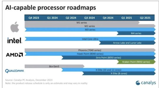
This is not the first time I have hearing of the Purwa die. Adroc has mentioned it before, but he said it's cancelled (!?). Also this Canalys report from last December....
Screenshot_20240327_085116_Gallery.jpg
It references a 10-core and 8-core part, in addition to the 12-core X Elite.

We can guess only one of them is a cut of the same die as X Elite, and only one of them will be called X Plus.
 

Ghostsonplanets

Senior member
Mar 1, 2024
338
544
96
I'd rather halve either the memory bus or SLC, not both. I have a suspicion that even the big Snapdragon X Elite SoC is having only a measly 6 MB SLC.
X Elite has a 6MB SLC? That's ridiculously low.

And, right. If the Snap X Plus do halve the memory bus, they need to keep the SLC intact. But my speculation is based on the fact QCOM loves to save costs even at expense of performance on mobile SoCs.
We can guess only one of them is a cut of the same die as X Elite, and only one of them will be called X Plus.
Agreed.
 

SpudLobby

Senior member
May 18, 2022
602
371
96
> Purwa is going to be called X Plus or something really close to that to differentiate it from the X Elite that is Homoa, and they are different dies.

This rules, and is very good for QC, because it means they’ll be doing another one at lower cost. Shaving it down to 8c with some lower clocks, a smaller Adreno could be substantial enough to warrant that.

Excited because it signals more seriousness than just one single SKU or two SKUs on one die. Ideally they don’t end up doing too many parts but this is good.

I assume it’s

X elite/X Pro same die

And then X Plus is the separate 6/8c die.
 

SpudLobby

Senior member
May 18, 2022
602
371
96
X Elite has a 6MB SLC? That's ridiculously low.
Fwiw the M stuff is still only 8MB and so is LNL.

Also we don’t know that it’s 6MB. We just know they’ve said it has 42MB of cache where they highlighted the cores on the chip and we know they have 3 clusters of 12MB of L2, for 36MB of L2. That’s included, the question is what is the 6MB: is it L3 or SLC, or is it the L1 they’re talking about.

It’d entirely possible it’s the L1 and they have 512KB of it, for 6MB total across 12 cores. The leaks had them having some L3 and SLC both fwiw, and I promise you the L1 is bigger than Arm’s cortex or Intel/AMD stuff currently, because of how big that shared L2 is.
And, right. If the Snap X Plus do halve the memory bus, they need to keep the SLC intact. But my speculation is based on the fact QCOM loves to save costs even at expense of performance on mobile SoCs.

Agreed.
It won’t be halved. I doubt that. Even the 7 series now has a 64-bit bus in phones. So no.

If they’re spending on an N4P die for the X Plus then yeah it’ll have a 128B bus if they want it to be even a more affordable premium part.
 

SpudLobby

Senior member
May 18, 2022
602
371
96
My speculation:

Snap X Plus => Targeting mainstream <$1000/$800 laptops

- 6 - 8C Phoenix Cores | 2P "Turbo Boost" cores + 6P Lower Clocked and reduced L2 cache. Or 2/4P Phoenix Cores + backported 4E Phoenix M cores
- 768/1024 ALU GPU. Based on Adreno 732 or Adreno 730 GFX IP
- NPU 45 TOPs
- Halved SLC and memory bus (64-bit LPDDR5X 8533)
- Targeting 10 - 15W for fanless or fanned laptops.

Target goals: Undercut AMD Kraken Point and Intel Lunar Lake while offering Apple M series of perf/W for mainstream consumers and beating LNL/KRK TTM by 2/3Q.
No memory bus halved, they can’t get away with that and won’t anyway for the reasons I explained, it doesn’t make sense and even 7 series phone SoCs have it now. Will bet the farm against that for a part like this from Qualcomm.


But I think a 4+4 style die with reduced clocks on both (as in, targeting lower clocks, not segmenting after the fact, so if they target 3.6GHz max it changes the physical design) and a smaller Adreno could save probably like 20-40mm of area.

Cutting down L2 too much wouldn’t be wise though, it will hurt efficiency profiles and a bit of IPC. I think they should keep it as it is mostly.
 

SpudLobby

Senior member
May 18, 2022
602
371
96
From Mr. Swords yes?

Not as insane as this:
View attachment 97261
The most efficient E-core in the world.
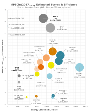
FWIW:

This comes up a lot. So Apple’s E Cores are indeed still the standard and it’s clear there’s an design component, probably in part also the humongous L1 (like 192KB total, 3x what most A7x cores use) and shared L2 cluster of 4MB, vs 256KB (like with the recent Dimensity 9300’s A7x) or 512kb of private L2 that’s very common on the A7x cores. They also don’t design for higher clocks in the phones, 2-2.4GHz max and 2.7GHz in Macs (area hit probably there), whereas even the 8 Gen 3 hits 3.2GHz for 3 A720s. Likely designing for 2-2.4GHz leads to a different phydes that plausibly impacts power at lower voltages.

Also, L1 & L2 are really just huge for energy efficiency.

Anyway, over the years when we compared A77’s, A78’s, and A710’s on crappier nodes *and* at higher clockspeeds — where voltage:frequency relationships dictate that higher voltages are used and then power blows up non-linearly, the A7x cores really got sloshed by the Apple E Cores albeit they were also still more performant.

You can see some of that here

IMG_9796.png

These days the E Core IPC has really improved, for one thing, without a bad power hit - though they’re also on N3B tbf.

For Geekerwan’s Spec results in the 8 Gen 2, the A715’s on N4 clocked to 2GHz for his tests, you see about the same performance as Apple but double the power from the A7x.

That’s still not ideal. But no one else has anything like these kinds of low power performances - and these are full SoC + package + DRAM + VRM power figures from Geekerwan.

AMD/Intel don’t really have anything like that and I seriously doubt Skymont in LNL will be this power efficient at this performance class.

Clocking down the X or Apple P cores can also get towards pretty good efficiency too, not as good as these but not far off from their higher clocked figures. You see this in the Geekerwan Geekbench graphs, you’re looking at 750 GB5 at .8-.9W (so the low power mode performance), it’s just a lot of area. X cores not far off, fairly similar.


My point?

A) Apple is still way ahead with their E Cores being both very performant for their size and energy efficient. They are by far the best, yes.

B). A7x stuff isn’t as far off as people think and could be improved likely easily.

If they wanted to, a 128kb L1 and 1MB L2 would make the A7x more efficient.

C) Apple and Arm Big cores if clocked down are still pretty efficient as shown by Geekerwan’s GB ST graphs.


D) assuming Qualcomm has cores that are similar to Apple and Arm’s big cores but closer to Apple’s, and they’re spending on area — such as with L2 and L1 — then doing e cores that are just cut-down P cores should prove pretty fruitful, and I wouldn’t be surprised if they can beat Arm’s current A7x stuff (which hasn’t changed too much so it’s possible the next one won’t be too crazy of an upgrade nor will they spend on area for L1/2) even if the energy is still worse higher than Apple.
 
  • Like
Reactions: Tlh97

FlameTail

Platinum Member
Dec 15, 2021
2,356
1,275
106
A recent news story came out that Google is going to be forcing Youtube AV1 playback on all Android phones, including the ones which don't have hardware accelerated AV1 decoding.

Those phones will have to software decode AV1 using the CPU, which would take a hit to battery life and performance of the device.

Now, a group of people are mad at Qualcomm (rightly so, arguably) due to the fact that Qualcomm is gatekeepers AV1 support for their non-flagship SoCs.

The Snapdragon 8 Gen 2, 8s Gen 3 and 8 Gen are the only chips with AV1 decode. Not even the recently released Snapdragon 7 Gen 3 has AV1 decode. Even egregious- the Snapdragon 7+ Gen 3 (which is cut of the same die as the 7s Gen 3), does not have AV1 decode, which clearly shows Qualcomm is artificially withholding support for AV1.

In contrast, Mediatek's midrange Dimensity 8000 series chips have AV1 decode, and so do all of Google's Tensor chips (which are used in the midrange Pixel A series phones). The Exynos 2100 and Exynos 2200 also had AV1 decode, whereas their Snapdragon counterparts, the 888 and 8 Gen 1 do not, in a rare W for Exynos
 
  • Like
Reactions: Tlh97

FlameTail

Platinum Member
Dec 15, 2021
2,356
1,275
106
Snap X Plus => Targeting mainstream <$1000/$800 laptops

- 6 - 8C Phoenix Cores | 2P "Turbo Boost" cores + 6P Lower Clocked and reduced L2 cache. Or 2/4P Phoenix Cores + backported 4E Phoenix M cores
- 768/1024 ALU GPU. Based on Adreno 732 or Adreno 730 GFX IP
- NPU 45 TOPs
- Halved SLC and memory bus (64-bit LPDDR5X 8533)
- Targeting 10 - 15W for fanless or fanned laptops.

Target goals: Undercut AMD Kraken Point and Intel Lunar Lake while offering Apple M series of perf/W for mainstream consumers and beating LNL/KRK TTM by 2/3Q.
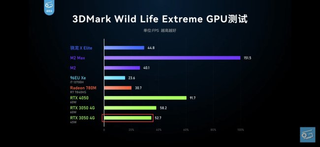
If Purwa has only half the iGPU of the X Elite, it will be too weak (vs competition).
Screenshot_20231031_174525_YouTube.jpg
Half the iGPU of X Elite means 22 FPS, which is even less than the OG Apple M1.

I doubt it will be able to keep up with 8 CU RFNA3.5 of Kraken Point or 8 Xe2 ARC GPU of Lunar Lake.
 

FlameTail

Platinum Member
Dec 15, 2021
2,356
1,275
106
But I think a 4+4 style die with reduced clocks on both (as in, targeting lower clocks, not segmenting after the fact, so if they target 3.6GHz max it changes the physical design)
I dont like this. I want it to have the same fmax as X Elite. That's one good thing about Apple Silicon- whether it's the base M chipvor the top tier M Ultra, the P-core runs at the same clock speed**
and a smaller Adreno could save probably like 20-40mm of area
That and the 4P+4E, i think they could get away with halving the memory bus.
Cutting down L2 too much wouldn’t be wise though, it will hurt efficiency profiles and a bit of IPC. I think they should keep it as it is mostly.
If it's a 4P+4E CPU, I see no reason to cut down the L2 in half. In X Elite, a 4P cluster has 12 MB L2. Keep it as it is. For the 4E cluster, it might be 4 or 6 MB of L2.

**I am aware that there was a slight clock speed difference between the base M chip and M Pro/M Max in the M1 and M2 generations. However, in the M3 generation they are all running at 4.05 GHz
 

FlameTail

Platinum Member
Dec 15, 2021
2,356
1,275
106
Fwiw the M stuff is still only 8MB and so is LNL.
LNL has an SLC?
It’d entirely possible it’s the L1 and they have 512KB of it, for 6MB total across 12 cores. The leaks had them having some L3 and SLC both fwiw, and I promise you the L1 is bigger than Arm’s cortex or Intel/AMD stuff currently, because of how big that shared L2 is.
512 KB L1 per core is monstrous. I doubt that, becuase if the cores indeed had 512 KB L1, I would think the IPC would be higher.

Also the possibility that the 6 MB is an L3 is bizarre, considering that Oryon CPU is a design that traces it's heritage to Apple's CPUs, which do not have an L3.

But maybe this makes sense for Qualcomm, if the CPU can't access the SLC. According to Andrei's findings (Anandtech article), in the Snapdragon 888, the CPU could not access the SLC, so the L3 functioned as effectively the LLC for the CPU. I don't know if Qualcomm is still doing this with recent chips like 8 Gen 2 or 8 Gen 3.
 

FlameTail

Platinum Member
Dec 15, 2021
2,356
1,275
106
The 8 core Purwa part sound like it's perfect for Chromebooks, in addition to <$800 Windows Laptops
 

SpudLobby

Senior member
May 18, 2022
602
371
96
LNL has an SLC?

512 KB L1 per core is monstrous. I doubt that, becuase if the cores indeed had 512 KB L1, I would think the IPC would be higher.
Lolololol.

No, it is not that simple. This, ceteris paribus in cache designs, impacts latency and there are a great many things that can impact IPC.

If it were that simple Apple would’ve absolutely done a 512KB L1 already — they can pay the area and have even *more* shared L2 to buoy them. They didn’t. Power it would impact however and could reduce the draw in some cases, albeit also possibly worse low load stuff.
Also the possibility that the 6 MB is an L3 is bizarre, considering that Oryon CPU is a design that traces it's heritage to Apple's CPUs, which do not have an L3.
Apple at one point did have an L3 for what it’s worth and it’s not a big deal if they do or don’t. The Apple hallmark is really about big L1, wide but dense core and shared L2 clusters.

And the leaks mentioned an L3 a while ago bro, that and an SLC both.

8MB of L3, 12MB of SLC.


It’s possible that’s wrong and they changed it except this person nailed everything else about it like the 3 12MB shared L2 clusters for 4 cores and the final cluster being lower clocks (which is true insofar as there are no prime cores).

He also got the display support largely right and Adreno 740, the frequencies for it, stuff like that.

I’d be surprised if the chip has just a 6MB SLC, it’s possible but it’s just a really odd choice. L3 I think is also slightly surprising if its there but not the same as just a 6MB SLC on a big leading chip — though to be fair again the shared L2 clusters are enough like, still.
But maybe this makes sense for Qualcomm, if the CPU can't access the SLC. According to Andrei's findings (Anandtech article), in the Snapdragon 888, the CPU could not access the SLC, so the L3 functioned as effectively the LLC for the CPU. I don't know if Qualcomm is still doing this with recent chips like 8 Gen 2 or 8 Gen 3.
They’re not, the SLC is accessible by the CPU now I believe.


The reason they did that at the time was it wasn’t worth the latency hit to DRAM because it was so small (4mb iirc) didn’t add enough. In this case 6MB for these cores I could see being similar. But why highlight “42MB of Cache” with the cores especially if the SLC isn’t for the CPU?”